


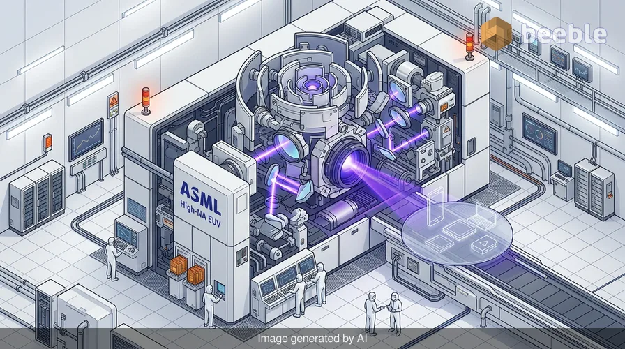
Inside the $400 Million Machines Finally Printing Your Next Smartphone Brain
If you are reading this on a smartphone or a laptop, you are holding a monument to human engineering that was, quite literally, carved by light. Every swipe, every app launch, and every video stream is powered by a silicon chip—a piece of digital crude oil refined into a masterpiece of logic. To find where these chips begin their life, we have to look past the sleek glass and metal in your hand and trace the supply chain backward, through the assembly lines in East Asia, past the massive fabrication plants in Oregon and Taiwan, and finally to a single, hyper-specialized company in the Netherlands: ASML.
For years, the tech world has been whispering about a "next generation" of chip-making equipment known as High-NA EUV. These machines are the most complex tools ever built by humans, costing roughly $400 million each—about the price of two Boeing 787 Dreamliners. This week, ASML Chief Executive Christophe Fouquet confirmed that the wait is nearly over. The first chips manufactured with these behemoths will arrive in months, not years. This isn't just an incremental update for gearheads; it is a foundational shift in how the devices you use every day will function in the near future.
Under the Hood: The Thinner the Line, the Smarter the Device
To understand why a $400 million machine matters, we have to look at how chips are actually made. In simple terms, chipmakers use a process called lithography, which is essentially a high-tech version of stenciling. They use light to "print" incredibly tiny circuits onto silicon wafers. For the last decade, the gold standard has been EUV (Extreme Ultraviolet) lithography.
Looking at the big picture, the goal is always to make those printed lines thinner. Thinner lines mean you can pack more transistors—the tiny on-off switches that do the "thinking"—into the same space. High-NA (High Numerical Aperture) is the next evolution of this process. If standard EUV is like a professional photographer using a high-end camera, High-NA is like that same photographer getting a lens with a much wider aperture. It allows for a sharper focus, letting the machine print features that are 66% smaller than what was previously possible.
Practically speaking, this means your future phone won't just be faster; it will be fundamentally more efficient. When transistors are packed closer together, electrons don't have to travel as far, which generates less heat and consumes less battery. This is the invisible backbone of modern life: the constant shrinking of the microscopic world to make our macroscopic world more interconnected and capable.
The $400 Million Gamble: Intel vs. TSMC
Behind the jargon of "numerical aperture" lies a massive corporate drama. Not every chipmaker is eager to hand over half a billion dollars for a single tool. In fact, a rift has opened up between the world’s biggest players.
Intel has been the most aggressive, effectively betting the company’s future on being the first to master High-NA. For Intel, this is an attempt to leapfrog its competitors and reclaim the crown of the world's most advanced chipmaker. Conversely, TSMC—the company that actually makes the chips for Apple and Nvidia—has been more cautious. Last month, TSMC executives suggested the machines were simply too expensive to justify right now. They believe they can still squeeze more performance out of older machines through clever design tricks.
On the market side, this creates a volatile dynamic. ASML’s Fouquet, however, remains resilient in his outlook. He argues that while the initial cost is eye-watering, these machines are designed to lower the "cost of patterning" over the long term. By printing a circuit in one pass instead of several, chipmakers can actually save money on materials and time once the technology is streamlined.
Why the AI Boom is the Real Driver
Curiously, the push for these machines isn't just about making your phone thinner. The real pressure is coming from the artificial intelligence explosion. AI is a tireless intern that requires massive amounts of data and processing power to function. To keep up with the demands of ChatGPT, Gemini, and the industrial AI applications being built today, we need chips that can handle unprecedented workloads.
| Feature | Standard EUV | High-NA EUV (Next Gen) |
|---|---|---|
| Cost per Machine | ~$150 - $200 Million | ~$350 - $400 Million |
| Resolution (Feature Size) | ~13nm | ~8nm (66% smaller) |
| Main Advantage | Current Industry Standard | Higher Precision, Fewer Steps |
| Lead Adopter | TSMC, Samsung, Intel | Intel, SK Hynix |
| Consumer Impact | Current Flagship Performance | Next-Gen AI & Battery Life |
Fouquet predicts that AI will keep chip sales rising by 20% annually. This puts ASML in a unique position. They are the only company in the world that makes these machines. If they can't build them fast enough, the entire AI revolution hits a systemic wall. While some fear ASML's production capacity might be a bottleneck, Fouquet flipped the script, suggesting that the real challenge lies with the chipmakers themselves. They have to expand their factories and find the capital to buy more of ASML’s products to keep the AI engine running.
What This Means for Your Wallet and Your Tech
For the average user, the arrival of High-NA chips in the coming months will initially be invisible. You won't see a "High-NA Inside" sticker on your next laptop. However, you will feel the effects in the next two to three years.
From a consumer standpoint, the bottom line is a trade-off between performance and price. As these $400 million machines become the industry standard, the cost of developing the world's most advanced chips will likely rise. We may be entering an era where the "pro" versions of gadgets become significantly more expensive than the base models, simply because the hardware inside them requires such a massive capital investment to produce.
Essentially, we are reaching the physical limits of how small we can make things using current materials. High-NA is a robust attempt to push those limits just a little bit further. For the user, this means that even as software becomes more demanding and AI becomes more integrated into every app, our hardware will have the headroom to keep up.
The Macro View: A Shift in the Global Order
Zooming out, the story of ASML and High-NA is also a story of geopolitics. Because these machines are so vital, they have become the center of a global tug-of-war. The ability to produce the smallest chips is now a matter of national security. When ASML says these chips are arriving "in months," they aren't just talking about gadgets; they are talking about the shifting balance of power in the tech world.
Ultimately, the arrival of these first High-NA chips marks the beginning of a new cycle. We are moving from the era of "making chips work" to the era of "making AI work at scale." Whether it's in a server farm or the pocket of your jeans, the light being pushed through ASML’s $400 million lenses is about to change the digital landscape once again.
As we look ahead, observe how your devices handle the next wave of AI updates. When your phone starts performing complex tasks locally—without needing to send data to the cloud—and your battery still lasts all day, you’ll know that a massive, Dutch-made machine somewhere in a sterile cleanroom is the reason why. Rather than just following the hype of the latest software, it pays to appreciate the invisible industrial mechanics that make the software possible in the first place.
Sources:
- ASML Official Press Statement, Q2 2026 Executive Briefing.
- Intel Foundry Services: Roadmap for 14A Process Nodes.
- TSMC Technology Symposium 2026: Cost-Benefit Analysis of Next-Gen Lithography.
- Imec Research Center: High-NA EUV Progress Report, Antwerp Conference.


See you on the other side.
Our end-to-end encrypted email and cloud storage solution provides the most powerful means of secure data exchange, ensuring the safety and privacy of your data.
/ Create a free account
