


Inside the New York lab where IBM is shrinking the world to seven angstroms
Every time you tap a screen to open an app, a silent army of microscopic switches flips to satisfy your request. These switches are transistors, and they have reached a size so small that atoms are the only remaining yardstick. IBM recently announced a breakthrough in this invisible world by producing a functioning 0.7 nanometer chip. To reach this scale, the company moved away from traditional flat designs and toward a vertical arrangement called a nanostack. This architecture packs nearly 100 billion transistors into a space no larger than a human fingernail.
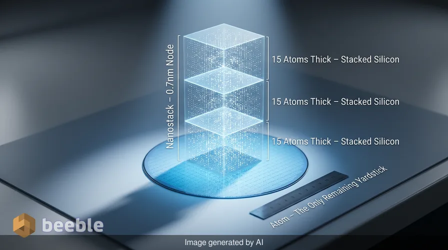
Stacking atoms to beat the limits of physics
The 0.7 nanometer chip starts with a raw silicon wafer. This wafer undergoes a process where light carves paths for electricity. In the new nanostack design, engineers stack three sheets of silicon to form a single transistor. Each sheet is only 15 atoms thick. These stacks sit on top of each other to save floor space on the chip. Saving space allows for a higher density of components. A higher density of components provides more processing power without increasing the physical size of the hardware.
Historically, chip progress followed a flat path. Designers laid transistors side-by-side like houses in a suburban neighborhood. As those houses became smaller, the industry ran out of land. IBM’s new approach is the digital equivalent of building a skyscraper. By staggering the transistors vertically, the company fits twice as many parts into the same area as its previous 2 nanometer design. This transition to 7 angstroms, which is 0.7 nanometers, marks the first time a company has successfully moved below the 1 nanometer barrier in a functional test chip.
The geometry of a 100 billion transistor chip
Under the hood, the nanostack architecture relies on a series of layers that are approximately five nanometers thick. A gap of nine nanometers separates each of these layers. For the average user, these numbers are difficult to visualize because they are smaller than a strand of human DNA. If a fingernail was the size of a city, one of these transistors would be the size of a small pebble on the sidewalk.
This density is foundational for the next generation of computing. Microchips are the digital crude oil of the modern economy, and their efficiency dictates how much we can accomplish with our devices. When you pack 100 billion transistors into a tiny area, the distance electricity travels becomes shorter. Shorter distances mean less heat and faster response times. The systemic shift toward vertical stacking is a practical response to the fact that we are reaching the physical limits of how small a single layer of silicon can be.
Choosing between battery life and processing speed
IBM says this new design gives manufacturers a choice. They can use the extra transistors to achieve 50 percent more performance or 70 percent greater energy efficiency. This is a trade-off that will define consumer electronics for the next decade. Practically speaking, a 70 percent jump in efficiency means your smartphone could go four days without a charge. Conversely, a 50 percent performance boost would allow mobile devices to handle complex tasks that currently require a desktop computer.
For most users, the energy efficiency is the more tangible benefit. Modern apps and AI features are volatile consumers of power. They drain batteries at an unprecedented rate because they require constant calculation. A chip that does more work with less electricity is a resilient solution to the problem of short battery life. This efficiency is also a matter of macro-level sustainability. Data centers consume massive amounts of power to run the internet, and a 70 percent reduction in their energy needs would have a systemic impact on global electricity demand.
| Metric | 2nm Nanosheet (2021) | 0.7nm Nanostack (2026) | Change |
|---|---|---|---|
| Transistor Count | 50 Billion | 100 Billion | 100% Increase |
| Performance Gain | Baseline | Up to 50% | Significant Improvement |
| Energy Efficiency | Baseline | Up to 70% | Major Reduction in Power |
| Architecture | Horizontal Nanosheet | Staggered Nanostack | Vertical Shift |
Bridging the gap between a lab and a factory
Turning a lab breakthrough into a product you can buy is a slow and expensive process. The path from the IBM research center in Albany to a consumer device involves several industry layers. First, the design must move to a foundry. Foundries are the massive factories that print chips on silicon. IBM does not own these factories. Instead, they partner with companies like Rapidus in Japan to bring these designs to market.
Looking at the big picture, the timeline for this technology is optimistic. IBM estimates five years for mass production. This means we might see 0.7 nanometer chips in premium laptops or phones around 2031. However, the industry is still working to master the 2 nanometer process. Rapidus plans to start 2 nanometer production in late 2027. Moving from 2 nanometers to 0.7 nanometers requires a complete overhaul of manufacturing equipment. The machines that etch these patterns use extreme ultraviolet light and cost hundreds of millions of dollars each. These costs eventually trickle down to the consumer in the form of higher prices for flagship devices.
The high cost of microscopic precision
On the market side, the cost of developing sub-1 nanometer chips is becoming a barrier for many companies. Only a few players have the capital to participate in this race. This concentration of power makes the supply chain more opaque and less decentralized. When only one or two factories in the world can make the most advanced silicon, any disruption at those sites affects the global economy.
From a consumer standpoint, this means that the gap between budget phones and high-end phones will likely widen. The premium tier will have access to 7 angstrom nanostacks with incredible battery life. The mid-range market will likely stay on older, cheaper nodes for longer periods. This is a cyclical pattern in tech, but the extreme difficulty of sub-1 nanometer manufacturing makes the divide more permanent.
What this means for your next device
In everyday life, the arrival of nanostack technology will change how we interact with portable tech. We are currently in a period where hardware performance has plateaued for many basic tasks. A smartphone from three years ago feels very similar to a smartphone from today. The 0.7 nanometer breakthrough breaks this plateau. It provides a scalable path for the next ten years of innovation.
For the average user, the "So What?" filter suggests two main takeaways. First, battery technology is not the only way to get longer phone life. If the chip uses 70 percent less power, the battery effectively becomes larger without changing its size. Second, the cost of staying at the cutting edge of technology is rising. As the engineering becomes more complex, the price of the final product reflects the billions of dollars spent on research.
Ultimately, the announcement from IBM is a signal that the age of silicon is not over. There was a fear that we could not go smaller than 2 nanometers without running into the chaotic behavior of subatomic particles. The nanostack architecture is a clever way to keep the industry moving forward. It uses vertical space to bypass the limitations of horizontal area. This development ensures that computers will continue to grow more capable for the foreseeable future.
Practical foresight for the digital consumer
Rather than waiting for a 0.7 nanometer phone next year, look at your current digital habits. The shift toward higher efficiency is a reminder that the most powerful tool in your pocket is a result of invisible industrial mechanics. As these chips become more powerful, they also become more specialized. When you shop for your next device, prioritize the energy efficiency ratings over the raw clock speed. The next decade of tech will be won by the devices that stay powered on the longest, not just the ones that calculate the fastest. Keep an eye on the production milestones from Rapidus and Intel. Their ability to move these designs from the lab to the factory floor will determine when this breakthrough actually reaches your hands.
Sources:
IBM Newsroom Official Press Release
IBM Research Blog Technical Deep Dive
Rapidus Corporation Manufacturing Roadmap 2027
SemiEngineering Analysis on Angstrom-Era Lithography


See you on the other side.
Our end-to-end encrypted email and cloud storage solution provides the most powerful means of secure data exchange, ensuring the safety and privacy of your data.
/ Create a free account
